Case Study: Micsig Gen3 SigOFITOptical Isolated Probe in Double-Pulse Testing of SiC MOSFET for Two-Level Inverters
In power electronics applications, DC‑AC conversion is widely used. The core function of an inverter is to convert direct current into alternating current. Compared with IGBT power devices, two‑level inverters using SiC MOSFETs usually feature higher switching frequencies and stricter drive design requirements. To ensure system performance and reliability, engineers typically perform double‑pulse testing to determine key drive parameters such as gate resistance and RC snubber circuits, and verify whether the drive design meets requirements.
Case Study: Micsig Gen3 SigOFITOptical Isolated Probe in Double-Pulse Testing of SiC MOSFET for Two-Level Inverters
In power electronics applications, DC‑AC conversion is widely used. The core function of an inverter is to convert direct current into alternating current. Compared with IGBT power devices, two‑level inverters using SiC MOSFETs usually feature higher switching frequencies and stricter drive design requirements. To ensure system performance and reliability, engineers typically perform double‑pulse testing to determine key drive parameters such as gate resistance and RC snubber circuits, and verify whether the drive design meets requirements.
Case Introduction
In a typical double‑pulse test, engineers need to measure key parameters of SiC MOSFETs including drive waveforms, voltage stress, and current waveforms, so as to optimize the drive parameter design of two‑level inverters. In practice, drive waveform measurement is a major challenge: it is necessary to observe the Miller‑plateau voltage in the drive waveform and the drive crosstalk voltage of the complementary device, to evaluate whether the design of the drive power supply, gate resistance, and snubber circuit is reasonable. This requires test equipment to have not only high bandwidth but also high common‑mode rejection capability.
SiC drive design is stricter than IGBT design, mainly in two aspects:
- Difference in drive voltage and threshold voltage
The threshold voltage (Vgs(th)) of SiC MOSFETs is lower, typically 2–4 V. Interference from test equipment on the drive signal can easily cause false turn‑on or even device destruction. Therefore, optical isolation probes are recommended for SiC drive testing. SiC MOSFETs have a typical drive voltage of +18 V/−4 V and are highly sensitive to overvoltage and undervoltage.
In contrast, the threshold voltage (VGE(th)) of IGBTs is usually 5–6 V, with a typical drive voltage of +15 V/−8 V, providing a larger design margin.
- Higher switching frequency and greater crosstalk risk
SiC MOSFETs switch at much higher frequencies than IGBTs. Under high dv/dt switching transients, the Miller capacitance (Cgd) injects displacement current into the gate:
- During turn‑off, this current can generate a positive voltage exceeding the threshold across the gate resistance, causing Miller false turn‑on.
- During turn‑on, high dv/dt couples to the gate through the Miller capacitance, creating negative voltage spikes that threaten gate‑oxide reliability and damage the gate.
This is the common crosstalk phenomenon in two‑level inverters.
Test Example
- Device Under Test: PCS power board from a company
- Customer Issue: Severe signal distortion when using a conventional high‑voltage differential probe, especially near the Miller plateau, making it impossible to evaluate the rationality of turn‑on/off resistance and RC snubber parameters.
The customer was measuring the voltage stress and drive waveform of Q2, as well as the crosstalk of Q1.
- CH1 (Yellow): Q2 Vce
- CH2 (Green): Q1 Vgs (crosstalk waveform)
- CH3 (Blue): Inductor current Id
- CH4 (Red): Q2 Vgs (drive waveform)

- Figure 1: Q2 Turn-on Moment
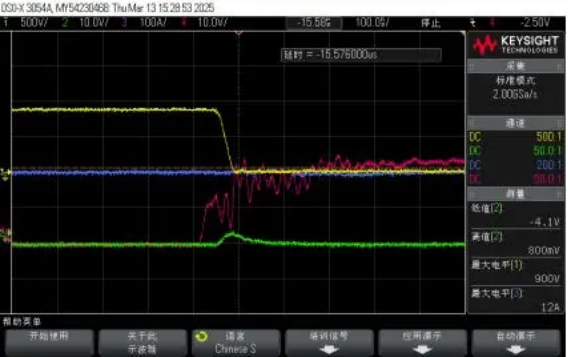
- Figure 2: Q2 Turn-off Moment
The waveforms show severe oscillations in the red drive waveform near the Miller plateau during Q1 turn‑on and Q2 turn‑off, which greatly hinders drive parameter tuning. Conventional high‑voltage differential probes have large parasitic parameters, introducing extra load and interference to the SiC MOSFET drive loop, and may even trigger gate false turn‑on in severe cases.
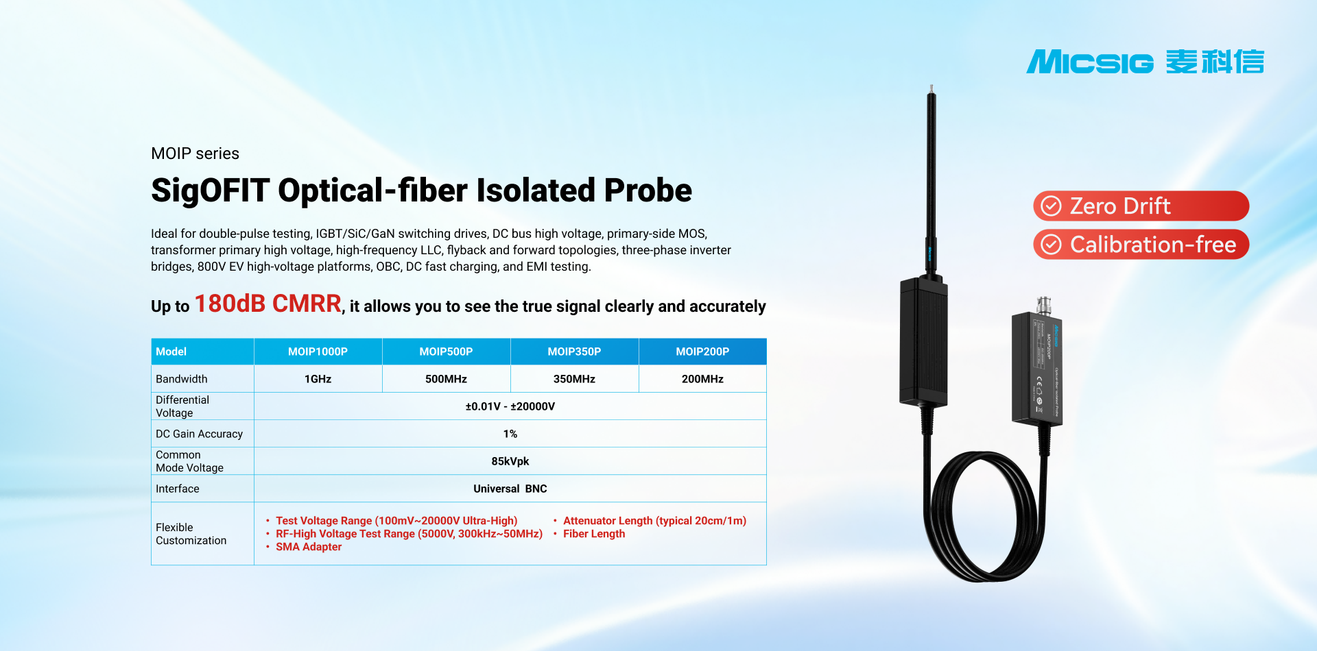
We then provided the customer with the Micsig 3rd‑generation optical isolation probe MOIP200P for a side‑by‑side comparison at the same test point:
- CH1 (Yellow): Q2 Vce
- CH2 (Green): Q2 Vgs (optical isolation probe)
- CH3 (Blue): Inductor current Id
- CH4 (Red): Q2 Vgs (high‑voltage differential probe)


Results show that the optical isolation probe delivers far better waveform quality than the high‑voltage differential probe, clearly revealing the Miller plateau of the SiC MOSFET drive, allowing the customer to tune drive parameters based on accurate waveforms.
⚠️ Note: When measuring SiC MOSFET Vgs drive waveforms in practice, do not connect two probes simultaneously at the same test point. Extra probes introduce parasitic parameters and mutual interference, leading to inaccurate waveforms. Measure separately and compare saved waveforms. This document is for performance comparison only.
Summary
The core advantage of Micsig 3rd‑generation optical isolated probes is their ultra‑high common‑mode rejection ratio (CMRR), which determines the probe’s ability to accurately extract weak differential signals under strong interference.
In SiC double‑pulse testing—especially when measuring the high‑side device in a half‑bridge circuit—we measure the tens‑of‑volts drive signal (Vgs) between gate and source, while the test point itself is on a rapidly switching high voltage (e.g., 800 V). This fast‑changing high voltage constitutes strong common‑mode interference.
The CMRR of conventional high‑voltage probes drops sharply at higher frequencies. When SiC devices complete voltage switching within tens to over a hundred nanoseconds, rich high‑frequency components are present. Differential probes fail to suppress strong common‑mode interference effectively, resulting in severely distorted, oscillatory Vgs waveforms that are almost unrecognizable.